|
Product Details:
|
| Product Name: | CZT Probe | Material: | CdZnTe |
|---|---|---|---|
| Operating Temperature: | -20℃~+40℃(standard) / -20℃~+70℃(customized) | High Voltage: | DC +80V~+100V |
| Window: | φ25mm | Signal Output: | Exponential Decay Signal, Tr<150ns |
| Connector Interface: | Five-core Cable | Power 0.3W Power Supply ±12V Output Impedance 50 Ω Operating Temperature -20℃~+40℃(standard) / -20℃~: | <1%@5.48MeV, 25℃ |
| Peak Drift (8 Hours): | <0.2% | ||
| Highlight: | Aerosol Detection Semiconductor Wafer,CZT Semiconductor Detector,Radon Detection Semiconductor Wafer |
||
Radon and aerosol detection CZT α-ray probe CZT Semiconductor Detector
The PDT-01A1 integrates CZT crystal and a low-noise charge-sensitive preamplifier circuit. The incident alpha particles are converted into exponentially attenuated signals of response amplitude, and directly input into the multi-channel energy spectrum acquisition system through the equipped five-core cable, high-voltage power supply and spectrometer amplifier.
Properties:
| Power | 0.3W |
| Power Supply | ±12V |
| Output Impedance | 50 Ω |
| Operating Temperature | -20℃~+40℃(standard) / -20℃~+70℃(customized) |
| High Voltage | DC +80V~+100V |
| Window | φ25mm |
| Signal Output | Exponential decay signal, Tr<150ns |
| Connector Interface | Five-core cable |
| Energy Resolution | <1%@5.48MeV, 25℃ |
| Peak Drift (8 hours) | <0.2% |
Advantage:
Room temperature working
High energy resolution
Quick response
Visible light environment
Applications:
Nuclear science & technology
Radon detection
Aerosol detection
Spectrum:
![]()
Compare with PIPS:
![]()
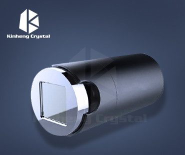
Product shots:
![]()
FAQ:
1.Q: Are you a factory manufacturer?
A: Yes ,we are manufacturer with 13 years experience in the scintillator crystal industry and supplied many famous brands with good quality and service.
2.Q:Where is your main market?
A:Europe, America, Asia.
Contact Person: Mr. Ivan. wang
Tel: 18964119345
Fax: 86-021-63063530