|
Product Details:
|
| Product Name: | SiC Substrate, SiC Semiconductor Wafer | Full Name: | Silicon Carbide Crystal Substrate |
|---|---|---|---|
| Chemical Formula: | SiC | Grade 1: | Production Grade |
| Grade 2: | Research Grade | Grade 3: | Dummy Grade |
| Contamination: | None | Size: | 10 Mm X 10 Mm (+/- 1mm) |
| Highlight: | Semiconductor Wafer 10 mm x 10 mm,SiC Wafer 10 mm x 10 mm,SiC Semiconductor Wafer |
||
Excellent thermal mechanical properties SiC Substrate SiC semiconductor wafer
Silicon Carbide (SiC) wafers are increasingly found semiconductor devices that were once dominated by silicon. Researchers have found that SiC semiconductor devices advantages over silicon wafers based devices include:
Properties:
| Item | 2 inch 4H N-type | ||
| Diameter | 2inch (50.8mm) | ||
| Thickness | 350+/-25um | ||
| Orientation | off axis 4.0˚ toward <1120> ± 0.5˚ | ||
| Primary Flat Orientation | <1-100> ± 5° | ||
| Secondary Flat Orientation |
90.0˚ CW from Primary Flat ± 5.0˚, Si Face up | ||
| Primary Flat Length | 16 ± 2.0 | ||
| Secondary Flat Length | 8 ± 2.0 | ||
| Grade | Production grade (P) | Research grade (R) | Dummy grade (D) |
| Resistivity | 0.015~0.028 Ω·cm | < 0.1 Ω·cm | < 0.1 Ω·cm |
| Micropipe Density | ≤ 1 micropipes/ cm² | ≤ 1 0micropipes/ cm² | ≤ 30 micropipes/ cm² |
| Surface Roughness | Si face CMP Ra <0.5nm, C Face Ra <1 nm | N/A, usable area > 75% | |
| TTV | < 8 um | < 10um | < 15 um |
| Bow | < ±8 um | < ±10um | < ±15um |
| Warp | < 15 um | < 20 um | < 25 um |
| Cracks | None | Cumulative length ≤ 3 mm on the edge |
Cumulative length ≤10mm, single length ≤ 2mm |
| Scratches | ≤ 3 scratches, cumulative length < 1* diameter |
≤ 5 scratches, cumulative length < 2* diameter |
≤ 10 scratches, cumulative length < 5* diameter |
| Hex Plates | maximum 6 plates, <100um |
maximum 12 plates, <300um |
N/A, usable area > 75% |
| Polytype Areas | None | Cumulative area ≤ 5% | Cumulative area ≤ 10% |
| Contamination | None | ||
Advantage:
1.High smoothness
2.High lattice matching (MCT)
3.Low dislocation density
4.High infrared transmittance
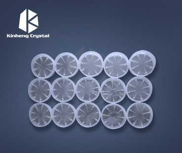
Product shots:
![]()
FAQ:
1.Q: Are you a factory manufacturer?
A: Yes ,we are manufacturer with 13 years experience in the scintillator crystal industry and supplied many famous brands with good quality and service.
2.Q:Where is your main market?
A:Europe, America, Asia.
Contact Person: Mr. Ivan. wang
Tel: 18964119345
Fax: 86-021-63063530