|
Product Details:
|
| Product Name: | CZT Semiconductor Wafer, CZT Substrate | Chemical Formula: | Cd0.96Zn0.04Te |
|---|---|---|---|
| CZT Substrate Size: | 20x20 +/-0.1mm Or Larger | CZT Structure: | Undoped Twin-free |
| CZT Thickness: | 1000 +/- 50 | Storage(transportation) Temperature: | -20℃~+40℃ |
| Storage(transportation) Humidity: | 20%~80%(non-condensing) | Packaging Environment: | Class 100 Clean Room, Vacuum Packed |
| Highlight: | MCT czt crystal,High Lattice Matching crystal wafer,High Flatness czt crystal |
||
High flatness high lattice matching MCT CZT semiconductor wafer
These substrates are high-performance wafers developed based on cadmium zinc telluride CZT crystals, which have excellent crystal quality and surface precision, and are the ideal epitaxial substrates for mercury cadmium telluride (MCT) infrared detectors.
Product features: high flatness, high lattice matching (MCT), low dislocation density, high infrared transmittance
Application areas: national defense, security, positioning, guidance
Properties:
| Crystal | CZT (Cd0.96Zn0.04Te) |
| Conductivity type | P type |
| Orientation | (211), (111) |
| Resistivity | >106Ω.Cm |
| Infrared transmittance | ≥60%(1.5um-25um) |
| (DCRC FWHM) | ≤30 rad.s |
| EPD | 1x10⁵/cm2 <111>; 5x10⁴/cm2 <211> |
| Surface Roughness | Ra≤5nm |
Advantage:
1.High smoothness
2.High lattice matching (MCT)
3.Low dislocation density
4.High infrared transmittance
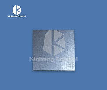
Product shots:
![]()
FAQ:
1.Q: Are you a factory manufacturer?
A: Yes ,we are manufacturer with 13 years experience in the scintillator crystal industry and supplied many famous brands with good quality and service.
2.Q:Where is your main market?
A:Europe, America, Asia.
Contact Person: Mr. Ivan. wang
Tel: 18964119345
Fax: 86-021-63063530