|
Product Details:
|
| Crystal: | CdTe | Growth Mehod: | PVT |
|---|---|---|---|
| Structure: | Cubic | Lattice Constant (A): | A = 6.483 |
| Density ( G/cm3): | 5.851 | Melting Point (℃): | 1047 |
| Heat Capacity (J /g.k): | 0.210 | Thermal Expans. (10-6/K): | 5.0 |
| Highlight: | High Energy Resolution CdTe Substrate,Cubic semi conductor wafer,PVT CdTe Substrate |
||
High energy resolution CdTe substrate CdTe Semiconductor Wafer
CdTe (Cadmium Telluride) is an excellent material candidate for high detection efficiency and good energy resolution in room-temperature nuclear radiation detectors.
CdTe substrate is an important II-VI group compound semiconductor material, and its crystal structure is sphalerite,with a direct transition energy band structure.
The production cost of CdTe thin film solar cells is much lower than other materials, and it is consistent with the solar spectrum, which can absorb more than 95% of sunlight. On the basis of extensive and in-depth application research, CdTe batteries have begun to scale industrial production from the laboratory research stage in many countries in the world.
Properties:
| Crystal | CdTe |
| Growth Mehod | PVT |
| Structure | Cubic |
| Lattice Constant (A) | a = 6.483 |
| Density ( g/cm3) | 5.851 |
| Melting Point (℃) | 1047 |
| Heat Capacity (J /g.k) | 0.210 |
| Thermal Expans. (10-6/K) | 5.0 |
| Thermal Conductivity ( W /m.k at 300K ) | 6.3 |
| Transparent wavelength ( um) | 0.85 ~ 29.9 (>66%) |
| Refractive Index | 2.72 |
| E-OCoeff. (m/V) at 10.6 | 6.8x10⁻¹² |
Advantage:
1.High energy resolution
2.Imaging and detection application
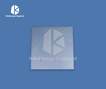
Product shots:
![]()
FAQ:
1.Q: Are you a factory manufacturer?
A: Yes ,we are manufacturer with 13 years experience in the scintillator crystal industry and supplied many famous brands with good quality and service.
2.Q:Where is your main market?
A:Europe, America, Asia.
Contact Person: Mr. Ivan. wang
Tel: 18964119345
Fax: 86-021-63063530