|
Product Details:
|
| Product Name: | CdTe Semiconductor Wafer | Full Name: | Cadmium Telluride |
|---|---|---|---|
| Chemical Formula: | CdTe | Thermal Conductivity ( W /m.k At 300K ): | 6.3 |
| Transparent Wavelength ( Um): | 0.85 ~ 29.9 (>66%) | Refractive Index: | 2.72 |
| E-OCoeff. (m/V) At 10.6: | 6.8x10⁻¹² | Surface: | One Side Polished / Two Sides Polished |
| Highlight: | CdTe Semiconductor Wafer,cdte substrate,Semiconductor Wafer High Imaging |
||
High Imaging and detection efficiency CdTe substrate CdTe Semiconductor Wafer
Cadmium Tellurium is a semiconductor and has recently found applications in the electronics industry. It was originally intended for use in the production of radiation detectors. Now we find Cadmium Tellurium usage in many other areas. Some of the applications are in the electronics, space applications, microelectronics, optoelectronics, optoelectronic devices, medical applications, as well as other areas. The reasons are many and varied.
Properties:
| Crystal | CdTe |
| Growth Mehod | PVT |
| Structure | Cubic |
| Lattice Constant (A) | a = 6.483 |
| Density ( g/cm3) | 5.851 |
| Melting Point (℃) | 1047 |
| Heat Capacity (J /g.k) | 0.210 |
| Thermal Expans. (10-6/K) | 5.0 |
| Thermal Conductivity ( W /m.k at 300K ) | 6.3 |
| Transparent wavelength ( um) | 0.85 ~ 29.9 (>66%) |
| Refractive Index | 2.72 |
| E-OCoeff. (m/V) at 10.6 | 6.8x10⁻¹² |
Advantage:
1.High energy resolution
2.Imaging and detection application
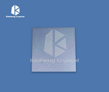
Product shots:
![]()
FAQ:
1.Q: Are you a factory manufacturer?
A: Yes ,we are manufacturer with 13 years experience in the scintillator crystal industry and supplied many famous brands with good quality and service.
2.Q:Where is your main market?
A:Europe, America, Asia.
Contact Person: Mr. Ivan. wang
Tel: 18964119345
Fax: 86-021-63063530