|
Product Details:
|
| Product Name: | Ge Semiconductor Wafer | Chemical Formula: | Ge |
|---|---|---|---|
| Size: | 10x3,10x5,10x10,15x15,,20x15,20x20,dia2” X 0.33mm Dia2” X 0.43mm 15 X 15 Mm | Thickness: | 0.5mm,1.0mm |
| Application: | Semiconductor Device , Microelectronics , Sensor , Solar Cell , IR Optics. | Advantage: | Excellent Crystallographic Properties And Unique Electric Properties |
| Crystal Structure: | Cubic | Lattice Parameter: | A=0.565754 |
| Thermal Conductivity: | 59.9 | ||
| Highlight: | 0.5mm Semiconductor Crystal Wafer,1.0mm ge wafer,Semiconductor Crystal Wafer |
||
Sensor Solar cell and Infrared optics applications Ge semiconductor wafer
Ge semiconductor wafer is an elemental and popular semiconductor material , due to its excellent crystallographic properties and unique electric properties , Ge wafer is widly used in Sensor , Solar cell and Infrared optics applications .
Properties:
| Growth Method | Czochralski method | ||
| Crystal Structure | M3 | ||
| Unit Cell Constant | a=5.65754 Å | ||
| Density(g/cm3) | 5.323 | ||
| Melting Point(℃) | 937.4 | ||
| Doped Material | No doped | Sb-doped | In / Ga –doped |
| Type | / | N | P |
| Resistivity | >35Ωcm | 0.05Ωcm | 0.05~0.1Ωcm |
| EPD | <4×10³∕cm2 | <4×10³∕cm2 | <4×10³∕cm2 |
| Size | 10x3,10x5,10x10,15x15,,20x15,20x20, | ||
| dia2” x 0.33mm dia2” x 0.43mm 15 x 15 mm | |||
| Thickness | 0.5mm,1.0mm | ||
| Polishing | Single or double | ||
| Crystal Orientation | <100>,<110>,<111>,±0.5º | ||
| Ra | ≤5Å(5µm×5µm) | ||
Advantage:
1.Sb/N doped
2.No doping
3.Semiconductor
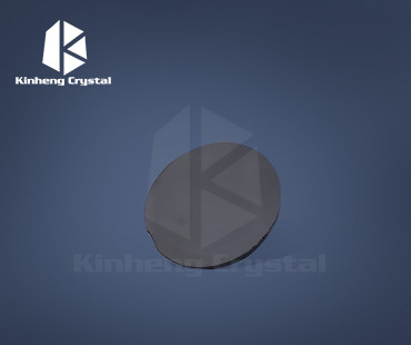
Product shots:
![]()
FAQ:
1.Q: Are you a factory manufacturer?
A: Yes ,we are manufacturer with 13 years experience in the scintillator crystal industry and supplied many famous brands with good quality and service.
2.Q:Where is your main market?
A:Europe, America, Asia.
Contact Person: Mr. Ivan. wang
Tel: 18964119345
Fax: 86-021-63063530