|
Product Details:
|
| Product Name: | PMN-PT Single Crystal Substrate | Chemical Formula: | Pb(Mg1/3Nb2/3)O3-PbTiO3 |
|---|---|---|---|
| Crystal Orientations: | (001), (110), (111) | Surface Finish: | Single Side Polished Or Double Side Polished |
| HS Code: | 3818009000 | Warranty: | One Year |
| Strength: | High Piezoelectric Coefficient, High Strain And Low Dielectric Loss | Available Thickness: | 0.5/1mm |
| Growth Method: | Bridgman Method | ||
| Highlight: | PMN-PTSemiconductor Wafer,High Strain Single Crystal Substrate,Low Dielectric Loss Semiconductor Wafer |
||
High strain and low dielectric loss PMN-PT Single crystal Substrate
As a novel kind of piezoelectric materials, relaxor-based ferroelectric single crystals exhibit ultrahigh piezoelectric performances, which surpass largely those of conventional PZTs piezoelectric ceramics. PMN-PT crystals, substrates and wafers with customized sizes, shapes, orientation, poling directions are available upon request.
Properties:
| Chemical Composition | ( PbMg 0.33 Nb 0.67)1-x: (PbTiO3)x |
| Structure | R3m, Rhombohedral |
| Lattice | a0 ~ 4.024Å |
| Melting Point(℃) |
1280 |
| Density (g/cm3) | 8.1 |
| Piezoelectric Coefficient d33 | >2000 pC/N |
| Dielectric Loss | tan d <0.9 |
| Composition | near the morphotropic phase boundary |
Advantage:
1.High smoothness
2.High lattice matching (MCT)
3.Low dislocation density
4.High infrared transmittance
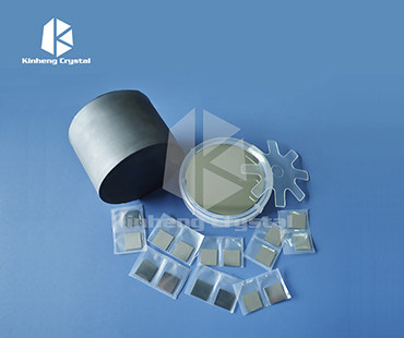
Product shots:
![]()
FAQ:
1.Q: Are you a factory manufacturer?
A: Yes ,we are manufacturer with 13 years experience in the scintillator crystal industry and supplied many famous brands with good quality and service.
2.Q:Where is your main market?
A:Europe, America, Asia.
Contact Person: Mr. Ivan. wang
Tel: 18964119345
Fax: 86-021-63063530